Component-to-System Level Packaging Workshop –
Addressing Integration Challenges for Automotive and Industrial Applications
July 2-3, 2025
Mercure Hotel MOA Berlin, Stephanstraße 41, 10559 Berlin, Germany
An GEA/IPC Technology Solutions Workshop supported by Research Fab Microelectronics Germany (FMD) with focus on APECS Pilot Line


The road to autonomous driving and the need for more electrified mobility have resulted in sizable changes for electronics such as semiconductors and batteries used in automotive applications. Smart homes and infrastructure, factory automation and preventive maintenance have driven significant advancements in industrial electronics too.
These applications demand significant system miniaturization through complex chiplet concepts and heterogenous integration solutions for processors, memories, power management along with sensors and MEMS, wireless and optical connectivity and other advanced communication components and systems.
Though assembly levels 0 and 1, with chip-package interaction challenges addressed, packaged device/components formation is enabled. Assembly levels 2 and 3 (board and system assembly) are indispensable from system level integration and final product/system performance points of view. With heterogenous integration solutions and miniaturization, the board as we know it today is partially moving inside the package, and System-in-Package (SiP) is created.
Advancements in compute and storage for automotive applications, sensor technologies with mmWave Radar, LIDAR, and other sensing techniques along with integrated power systems for EV with high voltage, high power components and modules are bringing new challenges to both, Component-Level Packaging (CLP) and Board/System-Level-Packaging (SLP). Power delivery, thermal management, assembly and reliability at component/system level demand innovative design approaches, materials and assembly processes for high reliability automotive and industrial requirements.
BE PART OF THE SOLUTION
The workshop is intended to bring together industry experts presenting and discussing CLP and SLP trends, requirements, challenges, solutions and the needs for guidelines/ standards desired for design, assembly, test, reliability and manufacturing from components (OSAT) and electronic manufacturing solutions (EMS) perspective.
Downloads
PLATINUM SPONSOR

GOLD SPONSOR

SILVER SPONSORS



SPONSORSHIP PACKAGES
ALL Sponsors’ Benefits:
- Promotion of your company as supporter of the workshop BEFORE the event: Logo and link to company website on the event website, the event flyer and brochure sent out in Mailings (size and positioning according to sponsorship level)
- Promotion of your company as supporter of the workshop DURING the event: Logo visibility during the workshop, the networking breaks and social event/ networking dinner ("Thanks to our Sponsors" Roll-up, mentioning in "Welcome Presentation", slide show during the breaks, table tents during coffee- and lunch breaks, and during networking dinner)
For more information and sponsorship booking, please contact:
Steffen Kröhnert, GEA/IPC Advisor & Lead Consultant Europe – Advanced Packaging Technology
steffenkroehnert@ipc.org / +49 (0) 172 7201 472

AGENDA
DAY 1 – Wednesday, July 2nd, 2025
“Problem-Statement-Day”
| Arrival of attendees on July 1st or July 2nd in the morning until noon. | Mercure MOA |
| Meeting Room is available from 09:00 am (setup, pre-meetings, networking) | MOA 3 |
| Registration open from 09:30 am – 1:30 pm | FOYER 1. OG |
| 11:30 am – 01:00 pm Standing Lunch + Networking | MOA 1-2 |
| Workshop Moderator: Steffen Kröhnert, Advisor & Lead Consultant Europe, Advanced Packaging Technology, GEA/IPC |
| Time | Topic | Room |
|---|---|---|
| 01:00 pm – 01:50 pm |
Session 1: Welcome, Scope and Introduction“Workshop Intent and Expectations” “GEA/IPC Introduction, Focus Areas, Collaboration” “Introduction and Overview of FMD and APEX” |
MOA 3 |
| 01:50 pm – 03:00 pm |
Session 2: Market Needs and Advanced Electronics Packaging Challenges“Advanced Packaging in Automotive Electronics” “Future Directions in Automotive Electronics: Challenges and Opportunities of Chiplet Technology“ “Challenges in heterogeneous integration for analog and mixed signal devices“ “Integration Challenges in Reliably Storing and Protecting Data in Industrial, Security and IoT Applications” |
MOA 3 |
| 03:00 pm – 03:30 pm |
Coffee Break + Networking | MOA 1-2 |
| 03:30 pm – 03:40 pm |
Sponsor-PitchesASE; Heller Industries; AT&S, Koh Young Europe, Resonac |
MOA 3 |
| 03:40 pm – 04:30 pm |
Session 3: Advanced Electronics Packaging Design and Concepts“Chiplet Center of Excellence – Introduction and Activities” “Designing Advanced Heterogeneous Packages: Shifting left for analyzing power delivery early on“ “The APECS Pilot Line as a new way of working with the FMD“ |
MOA 3 |
| 04:30 pm – 05:15 pm |
Day 1 – Panel: Components & System Integration Challenges for Sense/ Control,
|
MOA 3 |
| 05:15 pm – 05:45 pm |
Break to refresh and get ready for Social Event/ Networking Dinner | |
| 05:45 pm | Bus Pick-up at the Mercure Hotel MOA Berlin Short Sightseeing Tour Berlin – Tour ends at Networking Dinner Location |
Center of Berlin |
| 06:45 pm – 09:30 pm |
Social Event – Networking Dinner |
Classic-Remise Berlin |
| 09:30 pm | Bus Pick-up at the Event Location back to the Hotel | |
| 09:40 pm | Arrival at the Hotel MOA Berlin |
DAY 2 – Thursday, July 3rd, 2025
“Solution-Proposals-Day”
| Time | Topic | Room |
|---|---|---|
| 07:30 am – 08:30 am |
Morning Coffee and Snacks + Networking | MOA 1-2 |
| 08:30 am – 09:45 am |
Session 4: Materials, Assembly & Manufacturing, R&D Competencies I“Welcome and Recap” “Advanced Packaging Materials Innovation through Co-Creative Activities” “Solder As Known Good Interconnect (KGI) in Heterogeneous Integration” “Undermining the walls on the road to more advanced semiconductor technologies by novel IC substrate technologies” “Chip-on-Board (COB) in EMS – Industry Landscape, Challenges and Strategic Responses” |
MOA 3 |
| 09:45 am – 10:15 am |
Coffee Break + Networking | MOA 1-2 |
| 10:15 am – 11:15 am |
Session 5: Materials, Assembly & Manufacturing, R&D Competencies II“From Silicon to Systems: Optimizing the Opportunities Ahead” “Integration Challenges for Automotive and Industrial Applications from Neways Perspective” “Robust Chiplet Solutions for the Automotive and Industrial Sectors“ “Chiplet Packaging for Automotive“ |
MOA 3 |
| 11:15 am – 11:55 am |
Day 2 – Panel: Supply Chain Robustness and ChallengesPanelists: Hidenori Abe (Resonac), Andy C Mackie (Indium), Michael Goessler (AT&S), |
MOA 3 |
| 11:55 am – 12:00 pm |
Wrap-up and Next Steps Devan Iyer, Chief Strategist, Advanced Packaging, GEA/IPC |
MOA 3 |
| 12:00 pm – 01:00 pm |
Standing Lunch Break + Networking | MOA 1-2 |

Steffen Kröhnert
President & Founder,
ESPAT-Consulting
Advisor & Lead Consultant Europe, Advanced Packaging Technology,
Global Electronics Association
October 2023 – June 2024, Senior Manager, Pack4EU-Project (Chips Joint Undertaking – Coordination and Support Action), SEMI Europe GmbH, Berlin Germany
Started ESPAT-Consulting in July 2019, until June 2019, worked for 22 years in different Semiconductor Packaging R&D, Engineering, and Management positions at large IDMs and OSATs in Germany and Portugal (Siemens, Infineon, Qimonda, NANIUM, and Amkor)
In 2016 founded and since chaired or co-chaired the European SEMI-integrated Packaging, Assembly, and Test – Technology Community (ESiPAT-TC), a special interest group in SEMI focusing on manufacturing in Europe
Authored or co-authored 23 patent filings and many technical papers in the field of Packaging Technology, Co-edited two textbooks about „Embedded and Fan-Out Wafer and Panel Level Packaging Technologies”
Active member of many technical and conference committees of IEEE EPS, SEMI, IMAPS
IEEE EPS Program Director Region 8 (EMEA) and member of Bord of Governors
Holds an M.Sc. in Electrical Engineering and Microsystems Technologies from the Technical University of Chemnitz, Germany

Matt Kelly
CTO, VP Standards & Technology,
Global Electronics Association
Matt is CTO and Vice President of Standards & Technology at the Global Electronics Association. He is focused on driving next generation technology advancements and supply chain transformation across the global electronics industry. Currently, he leads Standards Development and Technology Solutions groups within the Association.
Matt delivers influential research, thought leadership, and advocacy to industry and governments. He works with industry to develop next generation guidelines and standards for emerging technologies. His focus areas include advanced electronic packaging, component and system-level co-design, and factory of the future modernization.
Matt comes to IPC with over 20-years commercial industry experience; most of this time at IBM, holding several senior technology and engineering leadership positions within IBM Systems Division. His technical contributions include 25 patents, 100 publications, and numerous industry awards from NAM, ASM, SMTA, IPC, and IBM.
Matt is a licensed Professional Engineer with a degree in Chemical Engineering from McMaster University and holds an MBA in Strategic Management from Sir Wilfrid Laurier University.

Dr. Devan Iyer
Chief Strategist, Advanced Electronic Packaging, Technology Solutions,
Global Electronics Association
Devan Iyer joined IPC in March 2024 as a Chief Strategist for Advanced Electronic Packaging . Devan Iyer has more than 35 years of experience in component and subsystems design & technology , Engineering, Manufacturing and Business leadership . He has served as Senior Vice President of Business units at Amkor Technology and Corporate Vice President at Texas Instruments. He has also worked for Infineon Technologies & General Electric.
As R&D Director he also led industry consortia at Institute of Microelectronics in Singapore and at the Packaging Research Center Georgia Tech . in Atlanta in electronic packaging designs and technology.
Devan has served as Conference Chair and Technical chair for several IEEE conferences. and regularly gives invited and Keynote talks at International conferences . He has more than 250 technical publications and 35 patents to his credit.
Abstract:
Devan will address some of the challenges in Component and System Level Packaging as applied to automotive and industrial application. He will emphasize the need for developing design, assembly and reliability guidelines and standards in the emerging areas of Heterogeneous integration.

Dr. Stephan Guttowski
Managing Director, Business Office,
Research Fab Microelectronics Germany (FMD)
Dr. Stephan Guttowski studied electrical engineering at TU Berlin and subsequently earned a doctorate in the field of electromagnetic compatibility. This was followed by a postdoctoral position at Massachusetts Institute of Technology (MIT) in Cambridge, USA. After his return, he initially worked in the Electric Drives Research Laboratory of DaimlerChrysler AG before moving to the Fraunhofer Institute for Reliability and Microintegration IZM in 2001. At IZM, he was initially head of the Advanced System Development Group before taking over at the System Design & Integration department. From June 2017 to December 2020, he was Technology Park Manager for Heterointegration at the Research Fab Microelectronics Germany (FMD). Since January 2021, he has led the joint office of the Fraunhofer Group for Microelectronics and FMD.
Abstract:
As a cooperation between the Fraunhofer Group for Microelectronics and the Leibniz Institutes FBH and IHP, the Research Fab Microelectronics Germany (FMD) is the central point of contact for all issues concerning research and development in the field of micro and nanoelectronics in Germany and Europe. As a one-stop shop, FMD has been combining scientific excellence, application-oriented technologies and system solutions of the 15 cooperating institutes from the Fraunhofer-Gesellschaft and Leibniz Association into a customer-specific offering since 2017. The pilot line for “Advanced Packaging and Heterogeneous Integration for Electronic Components and Systems” (APECS) marks the next major leap forward in strengthening Europe’s semiconductor manufacturing capabilities and chiplet innovation as part of the EU Chips Act.
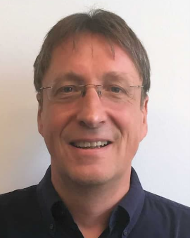
Andreas Grassmann
VP Package and Module Innovation,
Infineon Technologies AG
Andreas Grassmann is currently working for Infineon Technologies AG as Vice President for package innovation with strong focus on automotive and power electronics. He is in semiconductor industry since more than 30 years. He was working in various management position in R&D and semiconductor technology in Germany, UK, Austria, Malaysia and USA. He holds a PhD in Physics from the University of Erlangen.
Abstract:
Several trends are revolutionizing the car industry: e-mobility, the software defined vehicle and sophisticated assistance systems leading ultimately to autonomous driving. All these can only be realized by advancing automotive electronics. Based on system requirements we will discuss the usage of advanced packaging for advanced sensors, high power electronics for e-mobility and the need for chiplets and their packaging challenges for automotive computing.
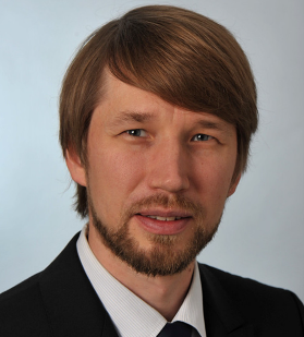
Pekka Sipilä
Head of Advanced Electronics Technologies,
Continental
Pekka Sipilä holds a Ph.D. in Electrical Engineering from the Technical University of Munich (TUM). With 20 years of experience in global research organizations across healthcare, aviation, energy and oil & gas sectors, he now since 2018 contributes to the automotive industry at Continental Automotive Technologies GmbH. His role at the central organization of Continental’s automotive segment involves managing research and innovation projects focused on advanced electronics solutions and methods, among others for topics around autonomous driving and central automotive HPCs.
Abstract:
This presentation provides an overview of the evolving landscape of automotive electronics, emphasizing the increasing complexity and performance demands driven by autonomous driving and smart vehicle expectations. Chiplet technology is highlighted as a promising solution for scalable, high-performance computing, offering advantages such as modularity, cost-efficiency, and design flexibility. The presentation also addresses the significant technical, economic, and ecosystem challenges that must be overcome for successful automotive integration. It concludes with insights from ongoing collaborative R&D efforts, including the PPP-CeCaS project, aimed at advancing chiplet adoption in the automotive sector.
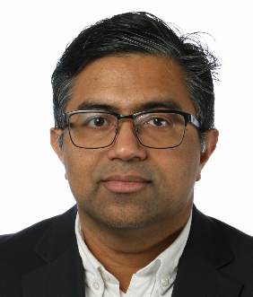
Dr. Rajesh Mandamparambil
Technical Director,
NXP Semiconductors
Dr. Rajesh Mandamparambil is a seasoned technology leader with over two decades of experience spanning academia, applied research, and industry innovation. He holds a Ph.D. in Photonics, and an MBA. He began his research career with a postdoctoral fellowship in optical sensing at City University London, followed by a pivotal role at TNO in the Netherlands, where he served as Senior Scientist and Program Manager, driving cutting-edge R&D in photonics and sensing technologies. Since 2016, he has been with NXP Semiconductors, where he currently serves as Technical Director. In this role, he leads pathfinding activities in semiconductor packaging, with a focus on millimeter-wave analog and mixed-signal device packaging.
Abstract:
This presentation explores key challenges in the heterogeneous integration of analog and mixed-signal devices for mmWave automotive radar and communication infrastructure. Topics include antenna co-design, signal integrity, thermal management, material compatibility, and long-term reliability. Real-world product examples will be used to illustrate how these challenges manifest in current mmWave systems. The talk aims to initiate a technical discussion to identify critical barriers and opportunities for innovation in high-frequency integration.

Torsten Grawunder
Senior System Designer embedded Solutions and System Architect,
Swissbit Germany AG
Torsten Grawunder is a hardware / security engineer. He studied physics of electronic components with a specialization in ASIC design in the field of communication Technology at the Technical University of Chemnitz. Since 2021 he has been working at Swissbit Germany AG in system design / embedded solutions in the APATS (Advanced Package and Test Solutions) department. Since then he has been creating / analyzing system concepts in pre-development for future NAND flash memory products and supervising the funding process of Swissbit Germany AG. For over two decades, he has played a key role in the hardware development of encryption devices for ISDN, ATM and Ethernet in various companies (Biodata AG, secunet Security Networks AG, Rohde & Schwarz SIT GmbH).
05/2021 Senior System Designer embedded Solution, Swissbit Germany AG
08/2018-04/2021 Cybersecurity Manager Product Development, Joyson Safety Systems Aschaffenburg GmbH
03/2027-07/2018 Lead Public Architecture & Strategy Manager, T-System International GmbH
04/2008-06/2016 Project Manager/System-Architect/Senior Expert HW-Developer, Rohde&Schwarz SIT GmbH
05/2005-03/2008 Head of department for high security hardware, secunet Security Networks AG
02/2001-04/2005 Technical managing director, Gateware communications GmbH
Abstract:
Within the Swissbit Group, Swissbit Germany AG operates as an IDM (Integrated Device Manufacturer) for Semiconductor Backends (APATS), offering a wide variety of storage form factors, from enterprise SSDs and µSD cards to heterogeneous bare DIE/chiplet integration in System-in-Package and even System-on-Package with Chiplets in BGA chip packages using advanced manufacturing. Swissbit’s core focus is on holistic data protection in digital storage media, including boot, firmware, application, data, and logging media, including cybersecurity challenges in the system architecture and chip co-packaging design process to meet EU regulatory requirements.
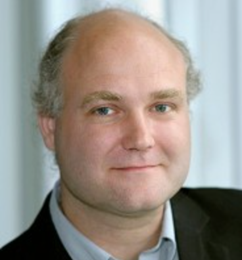
Andy Heinig
Head of Department Efficient Electronics,
Fraunhofer Institute of Integrated Circuits (IIS)
Andy Heinig was born in Dresden, Germany, in 1975. He received the Diploma degree in information technology from the Technical University of Cottbus, Cottbus, Germany, in 2006.,He then joined the Fraunhofer Institute IIS/EAS, Dresden, Germany. Since 2013, he has been leading the Working Group of Advanced Packaging, Fraunhofer IIS/EAS. In this position, he started several Saxony, German, and European research projects in the field of design and design automation for advanced packing. He is also working in different standardization groups, e.g., Si2. His research is in the field of assembly design kits and assembly design flows for advanced packaging where he has presented several papers at different conferences around the world.

Heiko Dudek
Business Development,
Siemens EDA (Siemens Digital Industries Software)
Heiko Dudek joined Siemens in 2021, M.Sc. Electrical Engineering, 26 years in EDA in various positions, including application engineering, R&D, services and technical sales, looking after solutions around advanced IC Packaging and signal and power integrity analysis.
Abstract:
This presentation explores the evolution of semiconductor design methodologies, focusing on early-stage power delivery optimization and advanced heterogeneous packaging solutions. The presentation highlights key elements for power delivery optimization, including data aggregation, core power modeling, and predictive analysis capabilities. The presentation demonstrates how integrated workflows combining thermal, electrical, and structural simulations support automated optimization processes, ultimately enabling faster turnaround times and enhanced productivity in advanced semiconductor package design.

Dr. rer. nat. Michael Töpper
Senior Expert for Technologies and Cooperation,
Research Fab Microelectronics Germany (FMD)
Michael Töpper studied chemistry at the University of Karlsruhe and received his doctorate in materials science from the Technical University of Berlin. He has been working in the field of assembly and connection technology for microelectronics since 1994, initially at the TU Berlin, then as a group leader at Fraunhofer IZM including a year at the University of Utah as an assistant professor and until 2021 as a business developer for the entire IZM. Today he represents the Research Fab Microelectronics Germany (FMD) as an senior expert.
Abstract:
By providing large industry players, SMEs, and start-ups with a facilitated access to cutting-edge technology, the APECS pilot line will establish a strong foundation for resilient and robust European semiconductor supply chains. Within APECS, the institutes collaborating in the Research Fab Microelectronics Germany (FMD) will work closely with European partners, to make a significant contribution to the European Union´s goals of increasing technological resilience, strengthening cross-border collaboration and enhancing its global competitiveness in semiconductor technologies. APECS is co-funded by the Chips Joint Undertaking and national funding authorities of Austria, Belgium, Finland, France, Germany, Greece, Portugal, Spain, through the “Chips for Europe” initiative. The overall funding for APECS amounts to € 730 million over 4.5 years.
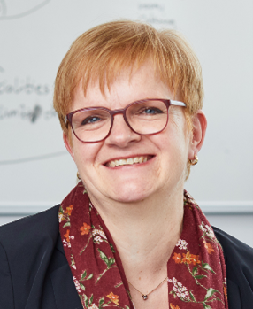
Dr. Elisabeth Steimetz
Director for EPoSS – the European Platform on Smart Systems Integration,
VDI/VDE Innovation and Technology GmbH
Elisabeth studied physics at RWTH Aachen, Germany with focus on semiconductor technologies and received her Ph.D. in physics from Technical University Berlin in the field of in-situ metrology of III-V materials. For more than 20 years she was active in the field of compound semiconductors (mainly LED / Laser fabrication and characterisation).
As a co-founder of LayTec GmbH (founded in 1999; company active in the field of in-situ and in-line metrology of thin film processes) she successfully built up the company and held the position of Director Strategic Marketing & Sales for 13 years. She is familiar with the semiconductor industries and the needs of SMEs.
In 2013 Elisabeth joined VDI/VDE Innovation and Technology GmbH as project officer for national and European funded projects in the field of Electronic Components and Systems. From 2014 until end of 2018 she was a German delegate in the public authority board of the EUREKA Clusters CATRENE and later PENTA, were she acted as national contact point as well.
Since 2019 she serves as Director for EPoSS – the European Platform on Smart Systems Integration – operated by VDI/VDE IT. In this position she was Chairperson for the ECS-SRA 2020 and ECS-SRIA 2021. She is lead delegate for EPOSS in the Private members Board and Governing Board of the Chips JU – the Pillar 1 activities of the European Chips Act.

Hidenori Abe
Executive Director / CTO for Semiconductor Materials,
Resonac Corporation
Hidenori Abe is CTO for semiconductor materials and Executive Director of Electronics Business Headquarters at Resonac. He leads R&D and strategy for electronic materials in semiconductors, substrates, and displays. Previously, Mr. Abe served as the head of the Electronics R&D Center and Packaging Solution Center, where he contributed to advanced packaging development through open innovation. Notably, in 2021, he directed the launch of JOINT2, a consortium targeting 2.xD and 3D packaging technologies.He received a master’s degree in chemical engineering from Tokyo Institute of Technology, Japan, and a master’s degree in the Executive MBA program from the University of Oxford, UK.
Abstract:
Resonac, a co-creation chemical company, has launched the evaluation platform „JOINT2“ with material, substrate, and equipment manufacturers to accelerate the development of cutting-edge packaging technology. In this presentation, we will explain the latest technology in panel interposer-related materials though this co-creation activity and our global strategy.

Andy C Mackie, PhD
Principal Engineer – Advanced Materials,
Indium Corporation
Overview:
* Internationally recognized Technology Thought Leader
* Strong continuous global business growth in advanced materials
* Vision and ownership of company technology roadmap
* Extensive experience living and working in Asia, Europe and the USA
* International keynote speaker (Asia/USA)
* Technical background in semiconductor fabrication, packaging and surface mount technology
* Developing strategy and executing through global teamwork
* Six Sigma methods drive decisions based on metrics
* Repeatedly recognized for outstanding electronics market insight, dependability and work ethic
* Insightful content creation
* Curiosity drives deep understanding and broad knowledge
Specialties:
* Turning early technology insights into business
* Global technical leadership and team building
* Strategy development and execution
* Returning loss-making businesses to profitability
Current Industry Associations:
* iMAPS Fellow
* Board of Directors of iNEMI
* Member of India Design, System, Semiconductor, Packaging (IDSPS) Consortium
* Technical leadership team of Automotive Electronics Council (AEC)
* Lead for Heterogeneous Integration Terminology Team (iMAPS)
* Past Chair of two IPC Task Groups: Sintering Materials (Group founder), and Solder Paste
* Member of IEEE: PELS, PES, TEMS, Photonics Societies
Alumnus of the UC Berkeley Product Management program (2015) and the RIT Kate Gleason College of Engineering Short Course in IC Processing (2003)
Philosophy:
– „A genuine leader is not a seeker of consensus but a molder of consensus“ – Martin Luther King
Work Ethic:
– „A day without work is a day without food“ – Ekai
Abstract:
Hybrid bonding / direct bonding (HyBo) remains of significant interest to those creating monolithic advanced packaged / heterogeneous integrated (APHI) devices. However, HyBo will likely remain a post-back-end of line process (BEOL) within wafer and system foundries, due to its sensitivity to particulates and specificities of CMP and surface conditioning. For OSATs and others seeking a more simplified approach, solder and the reflow process remain the primary means of creating a known good interconnect.
The presentation will cover how solder and low melting metals and metals alloys have evolved over the last 50 years, and the challenges ahead for assembly processes and reliability as new devices drive new power, performance, volume and cost requirements.”
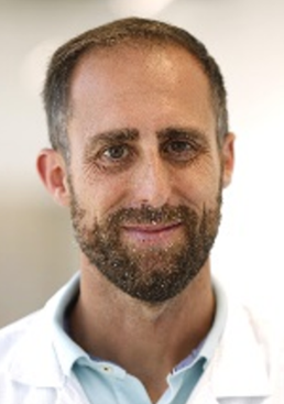
Michael Gößler
Head of R&D,
AT&S
Michael Gößler, MBA is Head of R&D at AT&S. He has been working for AT&S for 22 years. In his role he is focusing on the development of PCB and packaging technologies with a strong focus on embedding. He is a dedicated professional in program and project management with long history of developing new customers and technologies, passionate about new challenges and opportunities.
Abstract:
Over the past five years, the landscape of semiconductor system architecture has transformed dramatically. What was once a domain dominated by relatively simple single-chip packages has now evolved into intricate, heterogeneous multi-die and chiplet configurations. This shift has significantly increased the impact of packaging on both system performance and overall cost. And this is only the beginning.
This presentation highlights the critical challenges that must be addressed in the coming years to keep pace with these technological demands. It also explores how advanced packaging technologies and innovative substrate solutions can provide the foundation to overcome these hurdles. For Europe, this presents an exciting opportunity to reassert leadership and regain essential technological competencies for the future.
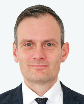
Stian Haugen
Chief Technology Officer,
Kitron Group
CTO with technical background within manufacturing, development and industrialization today holding a position within the senior management team of Kitron ASA.
More than 20 years of experience as a senior executive, manager or project manager for large international company, working in several global locations.
Specialties: Management, Project management, Development and Manufacturing, Industrialization and introduction of new products to production, Manufacturing Excellence driving performance, digitalization and automation.
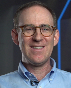
Dr. Bradford Factor
Senior Technologist,
ASE and USI Europe
Bradford Factor received his Ph.D. from Stanford University in Applied Physics in 1991. After performing research in polymer science, he began his career in the semiconductor packaging first at Intel in mid-1990’s. He subsequently worked developing optoelectronic devices at Corning in France. Since joining ASE in Europe in 2002, he supports the European customer base on both semiconductor packaging as well as electronic manufacturing services (EMS). Focus technologies include flip chip, wafer level, fan-out and 3D packaging, system-in-package as well as power packaging and modules, in particular for automotive applications. He is currently a board member of the IEEE EPS chapter in France and has received several patents and published several journal articles.
Abstract:
Semiconductors enable the electronics that have become omnipresent in modern society. Indeed, AI applications are increasingly permeating homes, workplaces, medical facilities, transportation modes, and more. This is creating great impetus for the industry to further evolve and deliver efficiencies, particularly related to energy and performance. Advanced packaging is playing a pivotal role. During his presentation, Bradford will draw from innovative breakthroughs and present advanced packaging technologies that foster highly complex integration and miniaturization requirements. He will also explore the tough challenges facing our industry, while discussing the collective effort to optimize integration technologies that deliver unprecedented efficiency spanning from silicon to systems.
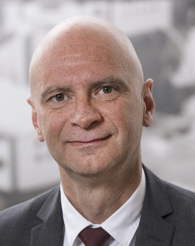
Oliver Maiwald
Global Sales Director, Microelectronics,
Neways Advanced Microsystems
Oliver Maiwald is an accomplished executive in the microelectronics and semiconductor industry, currently serving as Global Sales Director for Microelectronics at Neways Advanced Microsystems. With over 26 years of experience, he has built a distinguished career spanning R&D, product innovation, and global business leadership.
He began his career at Höft & Wessel, where he developed DECT hardware and software applications. He then joined National Semiconductor as a Product Application Engineer, where he supported a wide range of technologies — from RF and embedded software to full-system solutions — and developed deep technical and customer-facing expertise. This division later became part of Dialog Semiconductor, where Oliver transitioned into product marketing and played a pivotal role in advancing DECT integration into internet access devices.
At Dialog, he was the originator of DECT ULE (Ultra Low Energy) and an active contributor to DECT standardization at ETSI, helping to define key protocols for energy-efficient wireless communication.
In 2014, Oliver was appointed Managing Director of Sencio B.V., leading the company through strategic transformation and growth. Following the integration of Sencio into Neways Advanced Microsystems in 2024, he assumed his current role, where he is responsible for global sales strategy and customer engagement in advanced microelectronic packaging and system solutions.
Oliver holds a Master’s degree in Telecommunications Engineering from the University of Hannover, Germany.

Martin Haug
Global Head of Semiconductors,
Würth Elektronik eiSos GmbH & Co. KG
Martin Haug received the master degree in electrical and electronic engineering from the Ulm University of Applied Science, Ulm, Germany, in 1995.
After working for more than 15 years in the areas of automotive smart power ASIC design with ST Microelectronics and Bosch Semiconductor,
in 2014, he joined Würth Elektronik eiSos, Germany, where he holds the position of ‘Global Head of Semiconductors’.
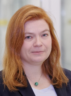
Dr. Tanja Braun
Head of Department, Group Manager Assembly and Encapsulation,
Fraunhofer Institute for Reliability and Microintegration (IZM)
Tanja Braun studied mechanical engineering at Technical University of Berlin with a focus on polymers and micro systems and joined Fraunhofer IZM in 1999. In 2013 she received her Dr. degree from the Technical University of Berlin. Tanja Braun is head of the department System Integration and Interconnection Technologies. Recent research is focused on Fan-out Wafer and Panel Level Packaging technologies. In 2021 she received the Exceptional Technical Achievement Award from IEEE Electronics Packaging Society (EPS) and the IMAPS Sidney J. Stein Award for her work in the field of Fan-out Wafer and Panel Level Packaging.
Tanja Braun is an active member of IEEE. She is member of the IEEE EPS Board of Governor (BOG) and is the IEEE EPS VP of Conferences.
Abstract:
The economic advantages of silicon scaling is gone. Only a limited number of foundries can afford the manufacturing of high-end nodes. Heterogeneous integration and therewith advanced packaging provides now an opportunity to achieve economic advantages lost with end of pure silicon scaling but also to enable new applications. Many options for the package including silicon interposers, Fan-out on substrate, and variations of 3D stacking approaches are seen as possible solutions. However, performance of current applications requires still more transistors, but industry also needs a new, more economical approach. Chiplets are the main solution to overcome this challenge.
Besides all the design aspects Chiplet packaging also holds quite some challenges and requires advanced packaging approaches especially with view to automotive application. The presentation will summarize different advanced packaging solutions as flip chip on organic, silicon or fan-out interposer and discuss key challenges as e.g. warpage and possible mitigation solutions.
Media- and Event Partners

